
purpose of a thermal relief in Pcb productions
In PCB production, thermal relief is an important design feature that ensures the proper functioning and reliability of a printed circuit board (PCB). It refers to the pattern used to connect heat-sensitive components to the larger copper planes on the PCB while managing and dissipating heat during soldering and operation. Without adequate thermal management, components can overheat, which may lead to failure or reduced lifespan of the device. In this article, we will explore the purpose of thermal relief in pcb production, how it works, and its significance in maintaining the integrity of a PCB.
Thermal relief involves designing specific copper trace patterns to help manage heat dissipation from components during the manufacturing and operational stages. Components such as power transistors, diodes, or voltage regulators generate significant heat when they operate, and if this heat is not efficiently dissipated, it can cause damage to the PCB and components. Thermal relief is the solution used in the PCB layout to prevent excessive heat buildup, ensure proper soldering, and promote long-term device reliability.
A typical thermal relief design incorporates a combination of copper pours (large areas of copper), heat sinks, and strategic placement of vias (small holes that conduct heat) to channel heat away from heat-sensitive areas. In this design, the copper pours are connected to components through small traces or pads that allow for controlled heat transfer without compromising the integrity of the PCB. The thermal relief pattern acts as a heat buffer and a controlled path for heat to dissipate away from critical areas.
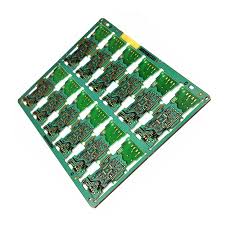
What is the purpose of a thermal relief in Pcb productions?
Thermal relief helps ensure a proper soldering process by controlling the flow of heat during PCB assembly. During soldering, especially in wave soldering or hand soldering processes, heat is applied to the PCB to melt solder and create electrical connections. If too much heat is absorbed by a component’s leads or pads, it may cause soldering defects such as cold solder joints or lifted pads. Thermal relief patterns, typically seen as spokes radiating from the pads to the surrounding copper planes, allow the pads to heat up gradually, making the soldering process more efficient and ensuring high-quality connections.
Heat dissipation is another critical role of thermal relief in PCB design. When certain components, such as power regulators or processors, generate heat during operation, it must be effectively managed to avoid component overheating. Copper planes are often used in thermal reliefs to dissipate heat evenly across the PCB. These planes absorb and spread the heat over a larger area, allowing it to dissipate more effectively and preventing localized hotspots that could damage sensitive components.
The main purpose of thermal relief is to prevent component damage due to overheating. Without an adequate thermal relief design, components that generate heat could overheat and lead to malfunction or permanent damage. By distributing heat efficiently across the board, thermal relief ensures that the components remain within their specified operating temperature ranges, thereby extending their lifespan and improving the overall reliability of the PCB.
In addition to thermal management, thermal relief also helps maintain the structural integrity of the PCB during manufacturing. Excessive heat during soldering can cause warping or thermal stress, especially in multi-layered or complex boards. Thermal relief helps mitigate this risk by preventing hot spots, ensuring that the board retains its flatness and overall structural stability. Proper thermal management is crucial in multi-layer PCBs, as uneven heating during soldering or operation can lead to delamination, where the layers of the PCB separate, compromising the board’s functionality.
Thermal relief typically involves connecting the component pad to the PCB’s copper plane using a set of thin traces or spokes, which create a controlled connection between the component and the copper plane. This pattern allows the pad to absorb heat from the soldering process or during operation gradually, instead of rapidly absorbing large amounts of heat, which could cause issues. The amount of copper surrounding the pad determines how efficiently heat can flow away from it.