
Challenges Faced During Rigid Flex
Rigid flex is used to create circuit boards that require bending, flexing, or folding. This technology replaces the need for extra connectors and cables to connect rigid components together and speeds up assembly, reduces costs, and increases reliability. However, when it comes to making a rigid flex PCB, there are several challenges that can arise during the process. Some of these include:
The transition zone is the region where a rigid area of a printed circuit board meets the flexible section. This area is prone to defects such as adhesive squeeze-out, protruding of dielectric materials, and crazing. To prevent these issues, designers should ensure that their CM uses low-flow prepregs for the rigid sections of the PCB, and that they extend the flex coverlay into this area.
Signal integrity is another common challenge when creating a rigid flex PCB. This issue is caused by improper stack-up that leads to impedance mismatching between the rigid and flexible sections of the board. To avoid this issue, designers should ensure that the layer-stackup is symmetrical and balanced with respect to copper distribution and impedance requirements. In addition, they should also pair signal layers with reference planes to minimize signal coupling and control impedance in flex areas.
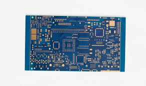
Common Challenges Faced During Rigid Flex
A good manufacturing process is an essential factor for ensuring the quality of rigid-flex PCBs. The fabrication process includes etching, drilling, and routing, and if any of these steps are done incorrectly, it can negatively affect the board’s performance. Rigid-flex PCBs often undergo specialized tests that are unique to their construction, including ESD and electromagnetic pulse testing and Moisture Resistance testing. These tests help to detect and fix any flaws that may affect the stability of the circuit board.
Rigid-flex PCBs are often subjected to mechanical stress during assembly, transportation, and use. This can cause solder joint failures if not addressed properly. During assembly, it is crucial to ensure that the correct solder paste is used on the traces and pins. In addition, the traces should be routed to avoid any sharp bends or corners.
Using a cross-hatched ground plane on a flex circuit can enhance its structural durability by providing a more resilient connection point with the rigid parts of the board. This design will also reduce the chance of damage to the copper during flexing or bending.
Routing traces on a flex circuit board that have sharp bend radiuses can lead to bending stress, which can result in copper trace thinning and fractures. To avoid this, designers should stagger traces on the flex circuit boards rather than having them overlap each other. This will distribute the bending stress and increase the longevity of the circuit. Adding dummy traces can further improve the structural integrity of the flex circuit boards. In addition, using larger coverlay openings can expose the edges of solder pads to physical stress, which can lead to shorts between solder joints. To avoid this, designers should choose smaller hole sizes and ensure that there is sufficient space between solder pads to reduce the risk of abrasion between these two components.