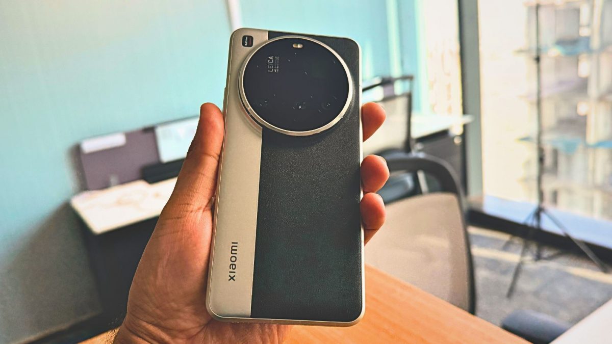
HDI PCB improve electrical performance
As the digital world becomes more complex hour by hour, the hardware that connects it is getting smaller and thinner. This trend has prompted the development of HDI PCB technology, which allows more interconnections to be placed in smaller areas, allowing for sleeker and lighter devices with enhanced performance. However, the intricate processes and specialized materials required to fabricate HDI circuit boards can result in elevated production costs, which may make them less attractive for price-sensitive market segments. Fortunately, manufacturers can utilize a number of strategies to lower manufacturing costs associated with HDI circuit boards without sacrificing quality and performance.
One of the primary ways to achieve cost savings is through reducing the size and number of layers in the board. This can be achieved by utilizing advanced materials and techniques, such as laser drilling and sequential lamination. Another method to reduce layer count is through the use of microvias, which are small holes that act as connections between layers. These can be drilled through the copper foil using laser technology, which is more precise and faster than traditional through-hole technologies.
In addition to reducing the overall board size, hdi pcb also incorporate a series of techniques that improve signal integrity. This includes routing differential pairs, which allow high-speed signals to travel along separate paths while minimizing crosstalk. In addition, the use of buried vias, skip vias, staggered vias, and stack-through vias can all be used to improve signal transmission speed and reliability.
How does HDI PCB improve electrical performance?
Increased component density: This allows designers to utilize more components in smaller spaces on the PCB, which in turn increases the amount of information that can be transmitted over the board. This is particularly beneficial in applications that require high-speed communication, such as mobile / cellular phones, touch-screen devices, laptop computers, digital cameras, and 4G network communications.
Reduced form factor: The asymmetrical structure of HDI circuit boards, which combine both copper and prepreg layers, helps to shrink the size of the overall board. This is especially important in compact electronics, such as handheld devices and wearables.
More efficient design: The asymmetrical structure of HDI PCBs allows for more complex and compact designs, which in turn decreases the amount of time it takes to bring a product to market.
Greater reliability: The asymmetrical structure of HDI boards and the use of microvias allows for a more robust design, which can withstand harsh conditions such as extreme temperatures and vibrations.
HDI PCBs are the norm in today’s modern electronic devices, from smartphones and tablets to medical implants and aircraft avionics. Their smaller sizes and improved electrical performance make them more desirable than their standard counterparts, allowing for sleeker, slimmer devices with better battery life and powerful processors. The streamlined design of HDI PCBs is also helping to revolutionize the medical industry, with implantable devices that are as small and discreet as possible while offering the functionality and reliability that is crucial for life-saving procedures.